Dev Board Schematic
The V853 Dev Board is designed by Allwinner's partner Sochip Technology based on the reference design provided by Allwinner.
This chapter will explain the schematic diagrams of several main components of the development board, so that it is convenient to quickly get started with the hardware information of the development board.
The hardware block diagram of the development board is as follows:
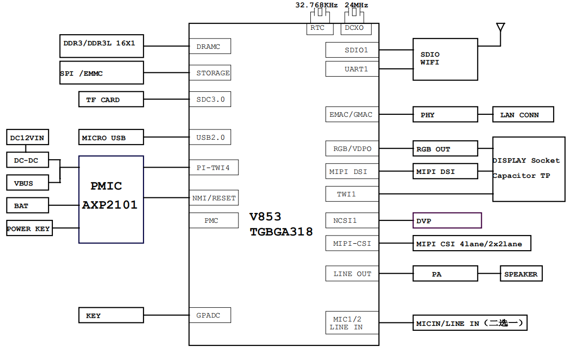
Schematic Introduction
GPIO List
This table is the allocation table of some important GPIOs of V853. > indicates another multiplexing of IO. For the complete GPIO allocation, please refer to the schematic diagram.
| GPIO GROUP | Use | Interface |
|---|---|---|
| PA[0:21] | MIPI CSI | Camera CAMERA FPC Connector |
| PC[0:11] | eMMC | Onboard eMMC |
| > PC[0:11] | SPF | Onboard SOIC16 (not weld) |
| > PC[0:6] | SPI0 | Onboard SOIC8 (not weld) |
| PD[0:22] | RGB(HV)LCD | RGB-LCD FPC Connector |
| > PD[1:7] | MIPI-DSI | MIPI-LCD Connector |
| > PD[13:14] | IR-CUT | Camera IR Filter Driver |
| PE[0:17] | DVP-CSI | Onboard 2x16p Connector |
| > PE[0:15] | RMII | Onboard IP101GR,100M ETH |
| > PE[8:15] | XR829 Bluetooth | XR829 Module |
| PF[0:6] | SDC0 | TF card slot |
| PG[0:7] | XR829 Wi-Fi | XR829 Module |
| PH[0:1] | UART 3 | UART3 pin array |
| > PH[0:1] | GPS | GPS 3.5mm Connector |
| PH[0:4] | I2S | I2S pin array |
| PH[5:8] | CTP | Touch Display FPC Connector |
| PH[9:10] | UART0 | UART0 pin array |
| PI[1:2] | PMU TWI | AXP2101 |
| PI[3:4] | TWI3 | 3-axis digital accelerometer (not weld) DA380B inertial sensor |
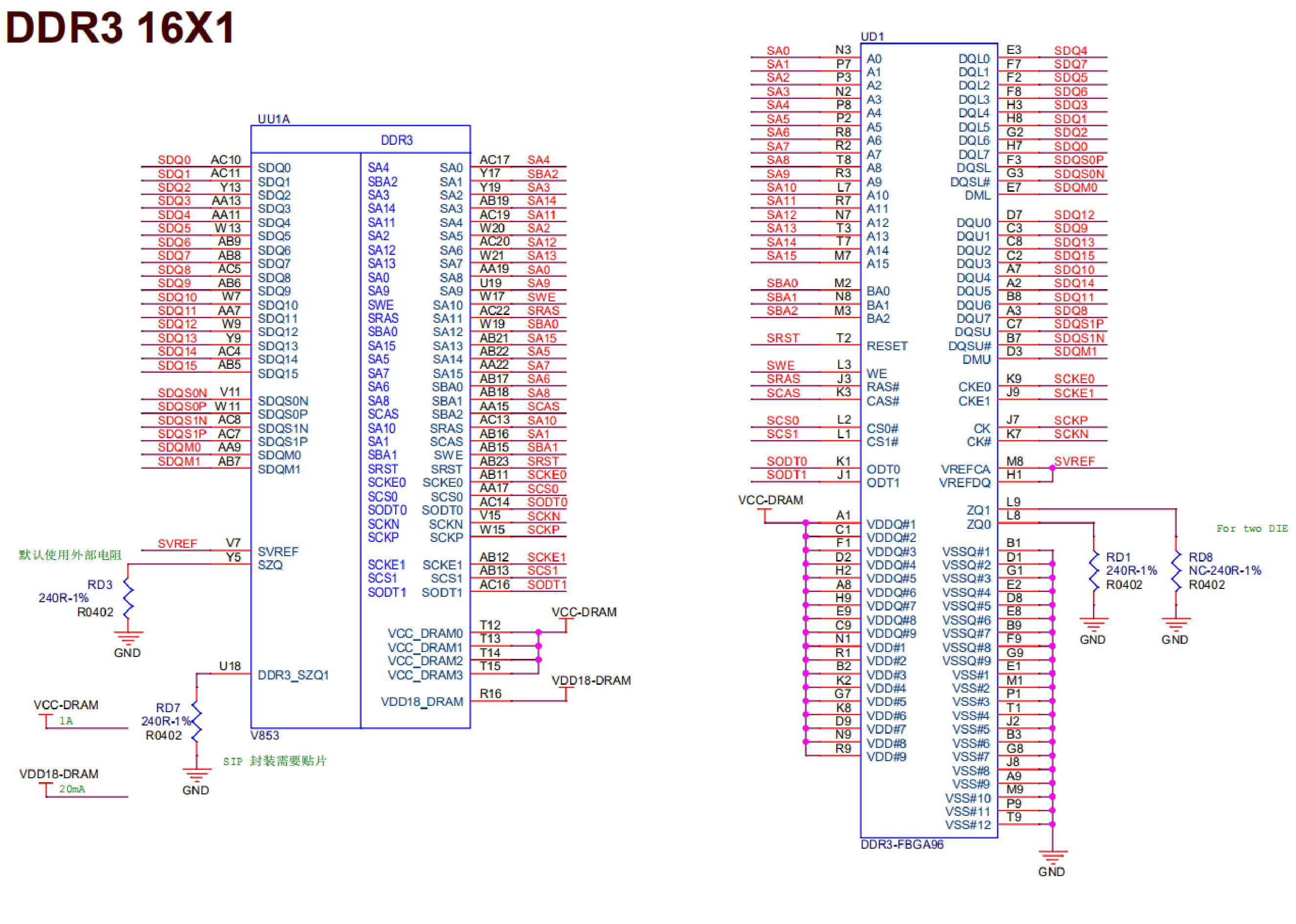
DRAM(DDR3)
The following figure is the schematic diagram of DRAM. The disorder of the SDQ signal lines on the particle side is the characteristic of DDR itself. The order of the SDQ lines in the group can be changed. There are two groups in total: the first group SDQ0- SDQ7+SDQSN/P0+SDQM0, the second group SDQ8-SDQ16+SDQSN/P1+SDQM1 This can facilitate the PCB wiring of the memory.
The V853 chip supports dual-stick DRAM, and also supports single-post dual-RANK DRAM, with a maximum of 8Gb.
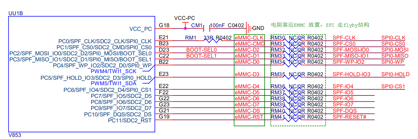
Memory(eMMC)
The memory of the development board is AT70B08G3 eMMC designed by Zhuhai Miaocun Technology, with a capacity of 8GB and running in 8bit mode.
The PC2 and PC3 pins are the BOOT SEL boot sequence selection pins, which can be started by pulling up or pulling down.
The development board has reserved pads for SPI NOR and SPI NAND, which can be soldered to the SPI NOR and SPI NAND memories supported by the V853 chip.
| BOOT SEL 0 | BOOT SEL 1 | 1 | 2 | 3 | 4 | 5 | 6 | 7 | 8 | Remarks |
|---|---|---|---|---|---|---|---|---|---|---|
| 0 | 0 | SPI NAND | SPI NOR(4 lane) | SPI NOR(1 lane) | USB FEL | |||||
| 0 | 1 | SPI NOR(4 lane) | SPI NOR(1 lane) | SPI NAND | USB FEL | fast boot use | ||||
| 1 | 0 | SDC 0 | SPI NAND | SPI NOR(4 lane) | SPI NOR(1 lane) | UART BRUN | USB FEL | |||
| 1 | 1 | SDC 0 | SPI NOR(4 lane) | SPI NOR(1 lane) | EMMC2 USR | EMMC BOOT | SPI0 NAND | UART BURN | USB FEL | default |
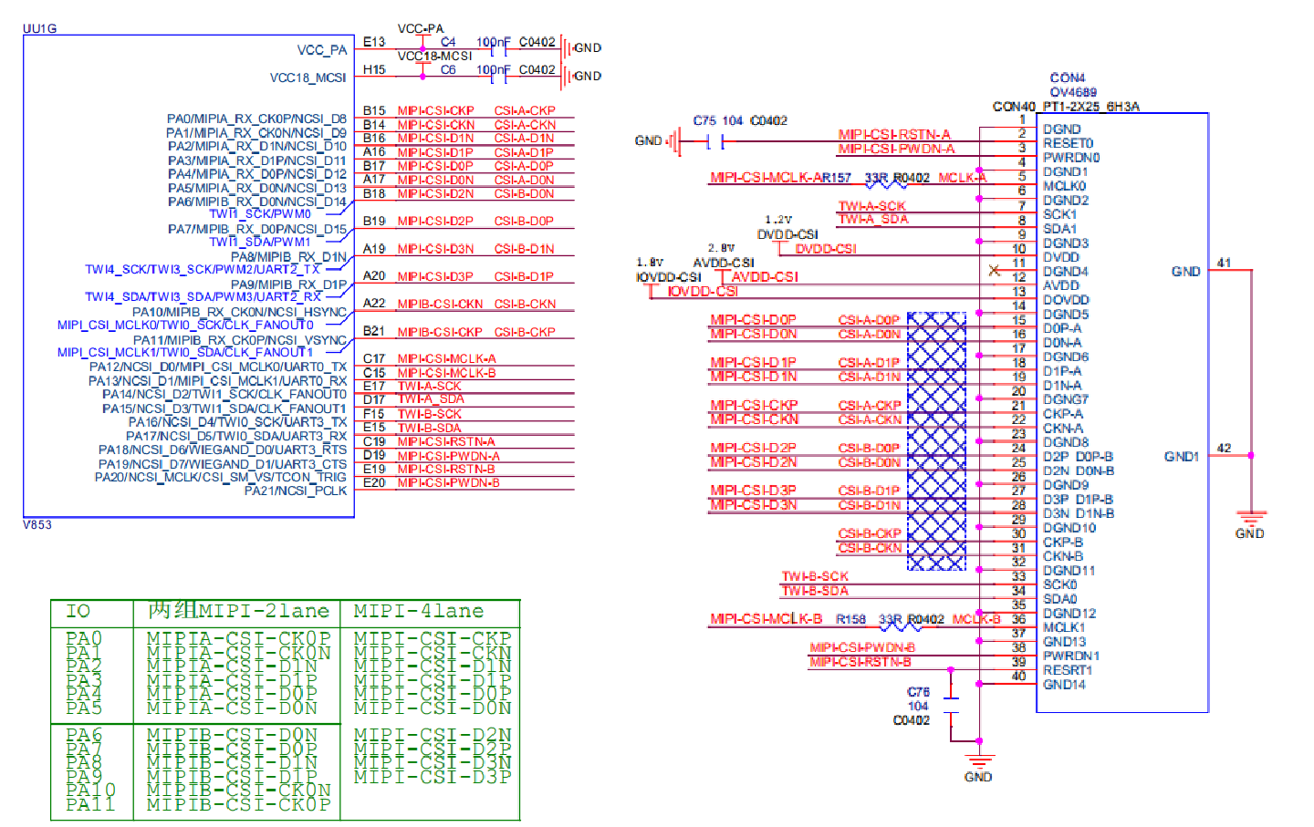
MIPI Camera(MIPI CSI)
The onboard 40Pin FPC connector of the V853 development board leads out all MIPI CSI resources, and supports dual 2 lane cameras and single 4 lane cameras. The development board provides a 1080P binocular camera solution by default, model: GC2063.
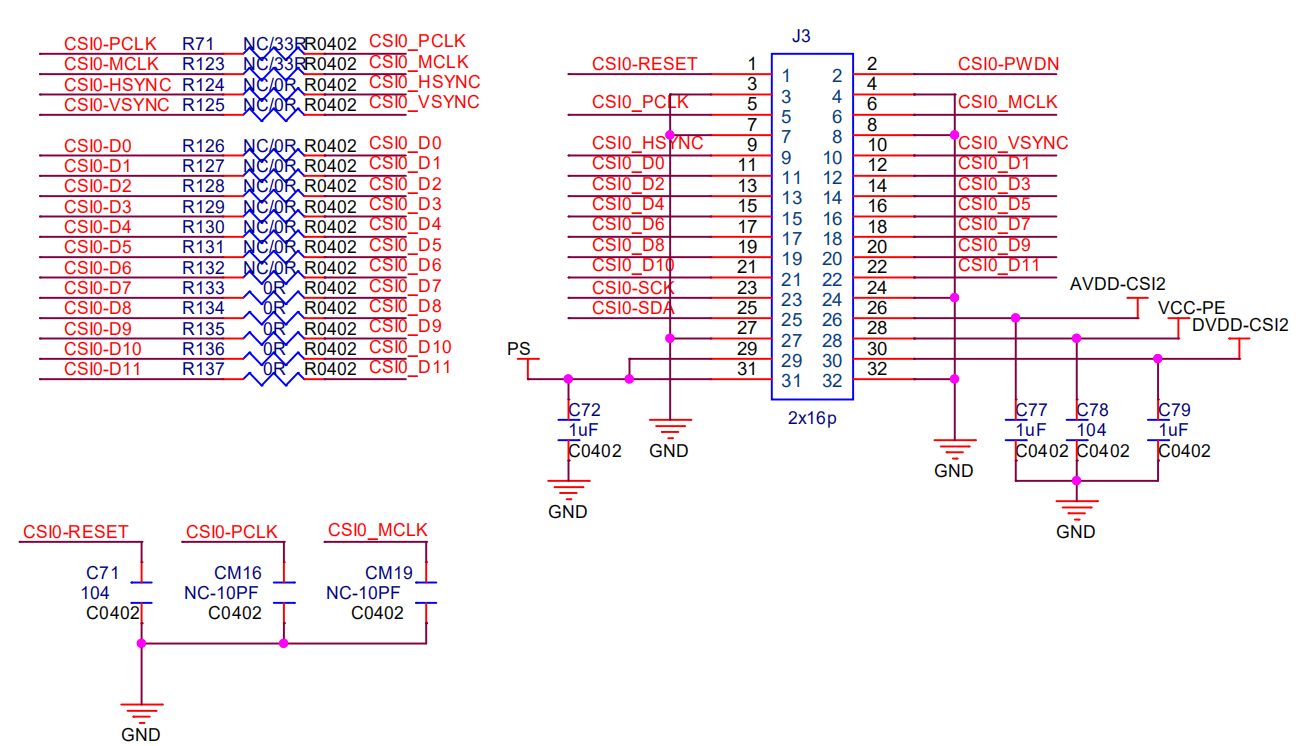
DVP Camera(DVP CSI)
The V853 dev board uses the female header to lead out the IO required by the DVP. Due to the multiplexing relationship of the PE interface, please pay attention to the multiplexing relationship when using it.
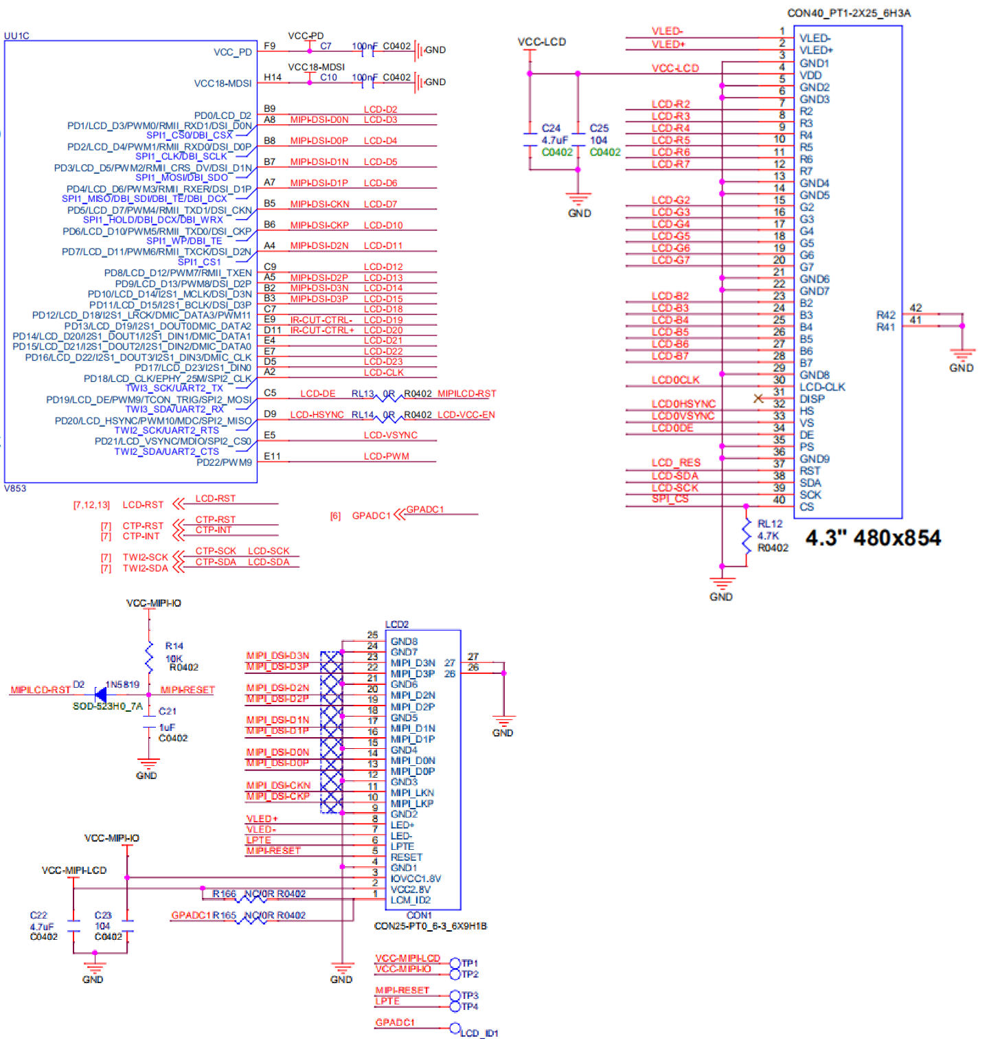
Display (LCD)
The V853 dev board is equipped with a 7-inch LCD screen with a corresponding capacitive touch screen.
The screen uses the MIPI DSI interface, which is connected to the corresponding MIPI LCD FPC connector of the board, and the touch screen is connected to the CTP interface.
At the same time, the development board also leads out the RGB666 FPC connector, which can be connected to the RGB screen (with TP)
Audio Input(MICIN、LINEIN)
The V853 dev board provides 2 channels of MIC audio input and LINE input. When using the LINE input, the MIC interface is multiplexed. Using the internal audio codec, you can also use the Inter-IC Sound (I2S) bus to connect an external digital codec to achieve microphone array and sound source localization.
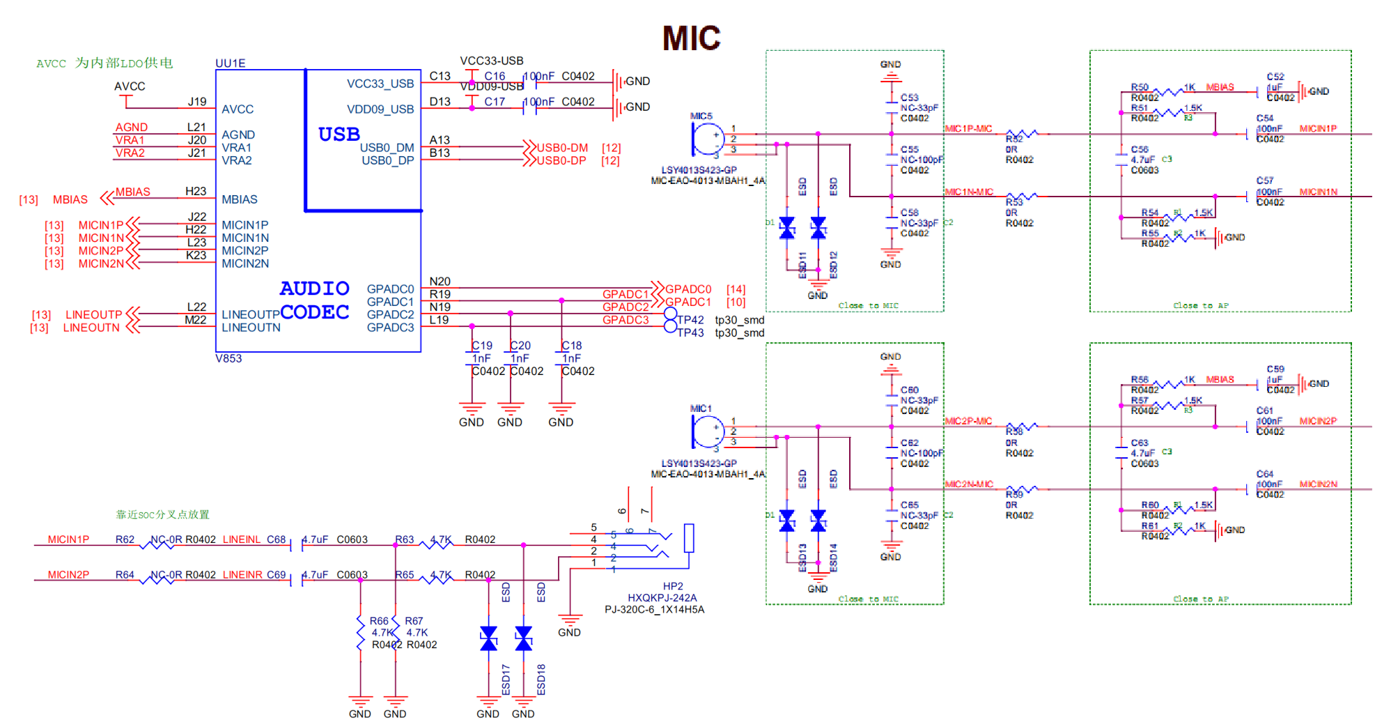
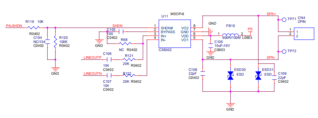
Audio Output(LINEOUT)
The V853 dev board provides a differential audio output interface, and uses the CG8302 power amplifier to connect to the speaker. The audio output uses the internal audio codec, or you can use the Inter-IC Sound (I2S) bus to connect an external digital codec to obtain better sound quality.
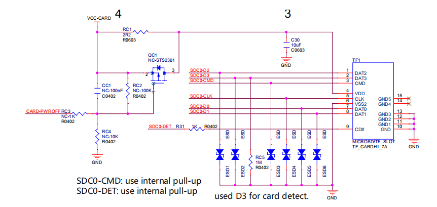
Micro SD Cart(TF Card)
Micro SD card (also known as TF card) Onboard self-elastic TF card slot, all pins of the card slot are protected by ESD devices.
The development board reserves a protection circuit for managing the power supply of the Micro SD card to prevent the low internal resistance Micro SD card from being burned. The development board does not mount this part of the protection circuit by default.
The SDIO interface used by the MicroSD card all use the internal pull-up of the chip, and no external pull-up circuit is required.
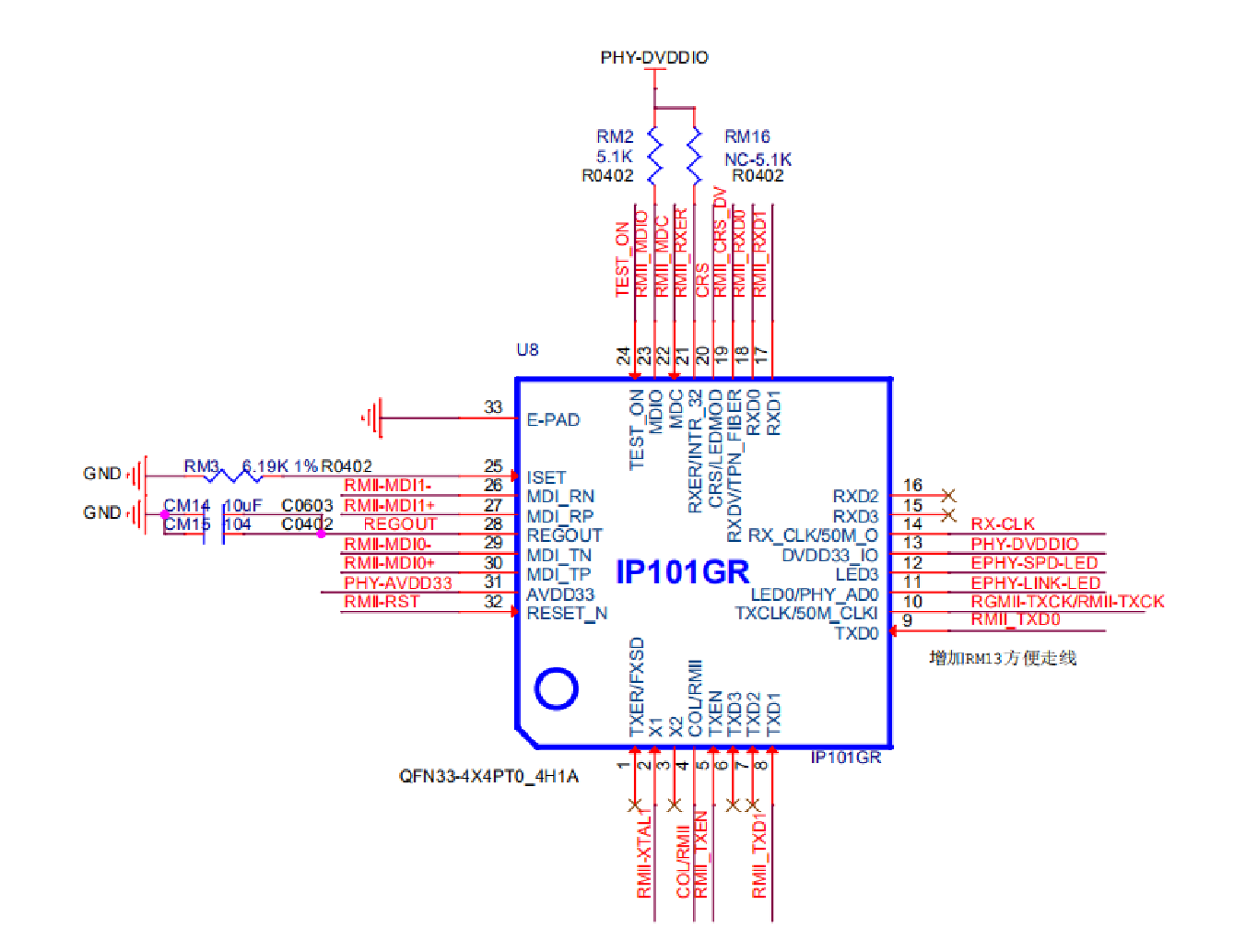
Network
The V853 dev board is equipped with an IP101GR Fast Ethernet transceiver, which can be connected to the Internet by connecting a network cable.
Wireless Network
The V853 dev board is equipped with XR829 Wi-Fi, Bluetooth module, supports 2.4G IEEE 802.11 b/g/n WLAN, Bluetooth v2.1/4.0/4.2. Wi-Fi communicates with V853 through SDIO bus, and Bluetooth communicates through UART.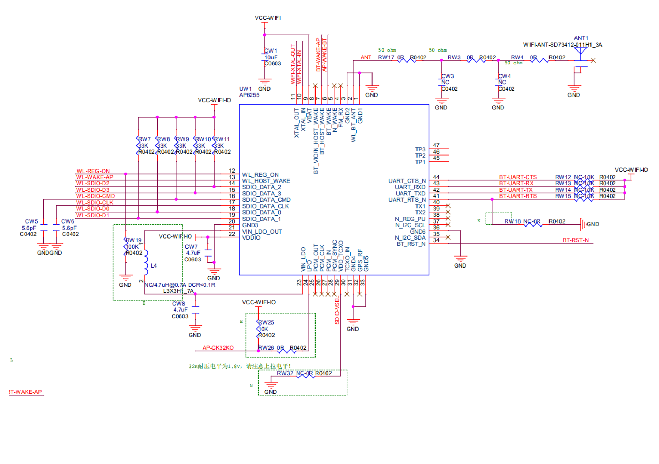
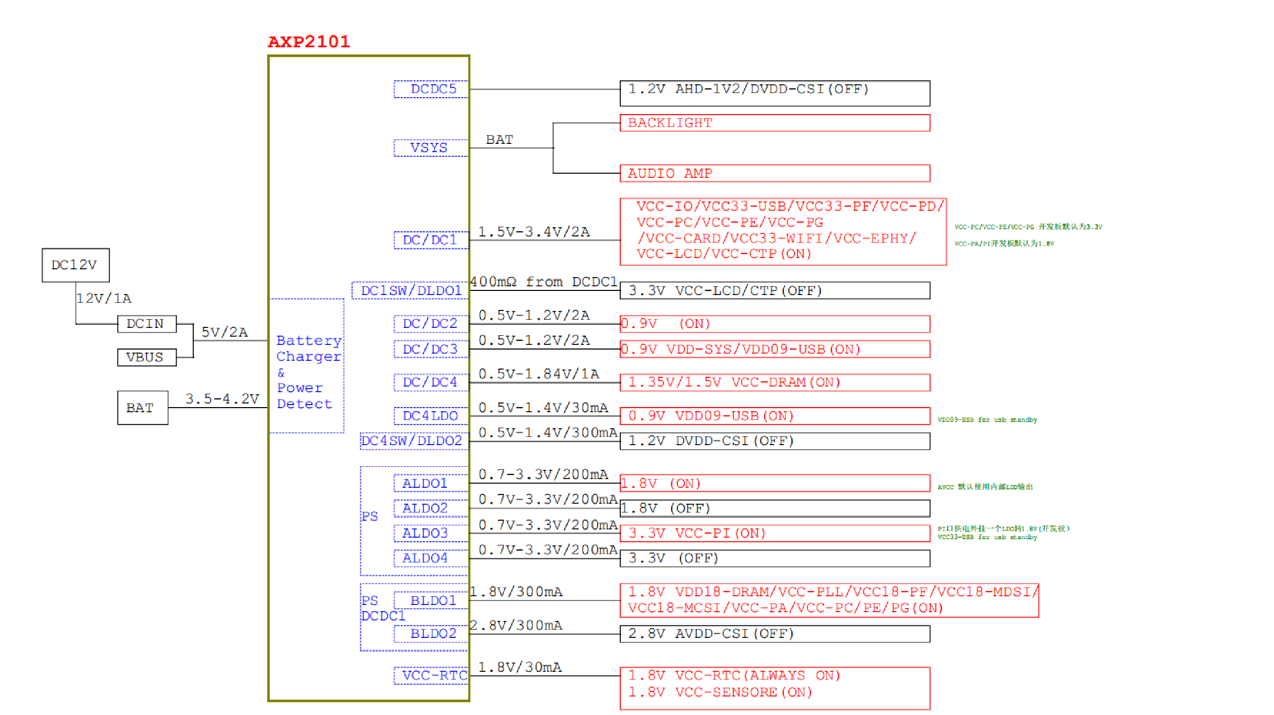
Poewr Tree
V853 dev board uses AXP2101 PMU, which is also self-developed by Allwinners, as the power management module. Can support DC 12V input, USB 5V input and battery input. It communicates with the V853 using the TWI bus.
AXP2101 is a general-purpose PMU, which can be adapted to a variety of chips and provides multiple power outputs. The power supply part that is not needed can be turned off.
The power output distribution is shown in the figure below (red is the power output enabled, black is the power output not enabled)
Button
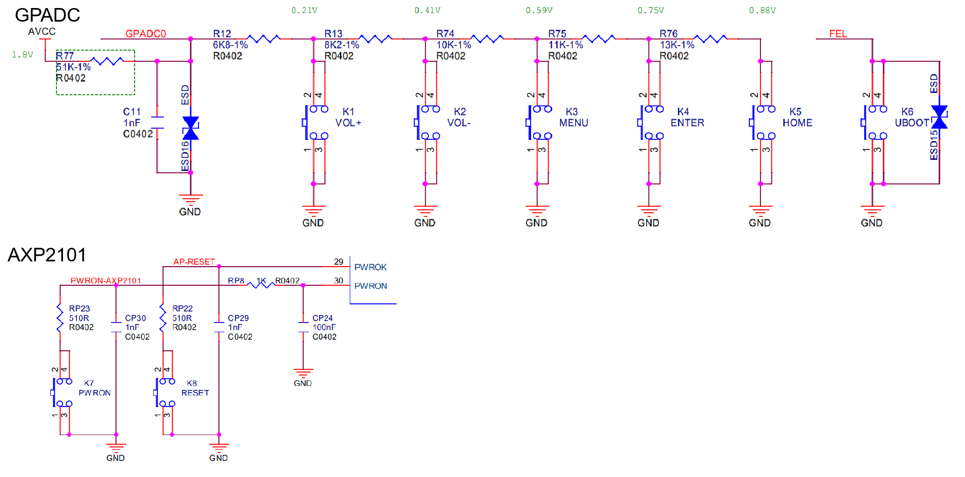
V853 开发板共有8个按键,其中按键 VOL+ VOL- MENU ENTER HOME 按键连接在 GPADC 上,通过识别当前ADC的电压识别按键键值。另外 UBOOT 按键连接到 V853 芯片上的 FEL 引脚,按下后可以进行刷机调试操作。
还有PWR 键与 RESET 键,是连接到 AXP2101 PMU上的,用于开机与 RESET 芯片。
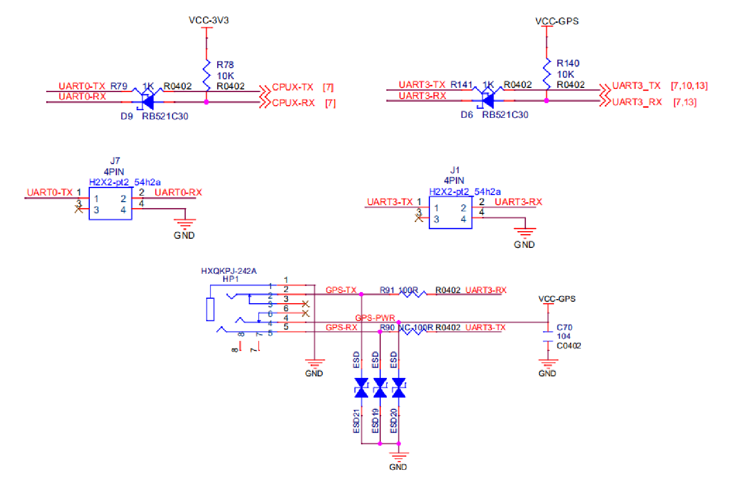
Serial Port (UART)
The V853 development board provides two independent UART debug ports, namely UART0 and UART3. By default, UART0 is configured as the Arm core serial port debug port, and UART3 is the E907 core debug port.
At the same time, UART3 can also be reused as the communication interface of GPS, and the on-board 3.5mm connector is connected.